What does 3D-MID technology offer?
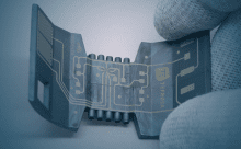
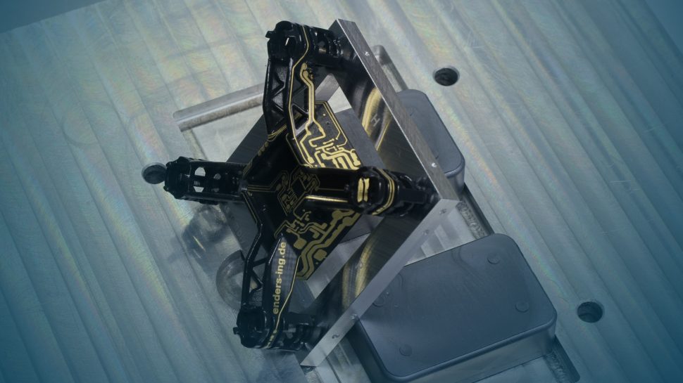
MID technology makes it possible to use three-dimensional plastic parts as circuit carriers for electronic or mechatronic assemblies. A special process is used to apply metallic conductive tracks to a specific substrate material (often plastic) to create three-dimensional assemblies that also serve as circuit carriers.
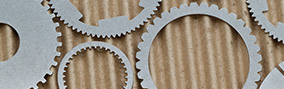
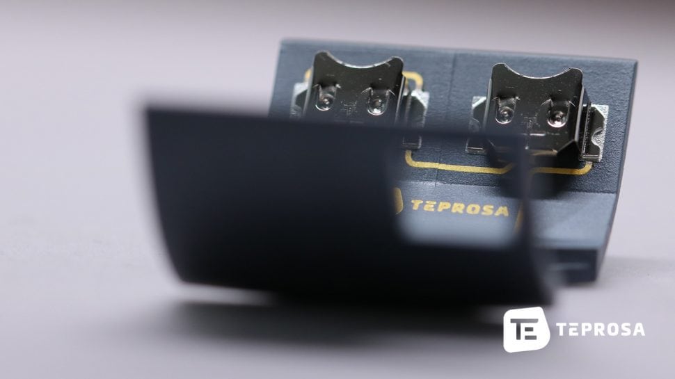
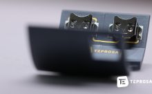
These spatial electronic assemblies are manufactured using 3D-MID technology and, compared with conventional assemblies, enable the integration of electronic, mechanical, fluidic, optical and thermal functions. The resulting additional benefits represent advantages that cannot be realized with two-dimensional circuit carriers (printed circuit boards).
As a full-service provider, TEPROSA offers you the entire manufacturing chain of 3D MID technology from a single source. If external processes are required to manufacture your MID, we will be happy to take over supplier management so that you can concentrate fully on your product.
We will be happy to advise you!
Our competencies lie in the manufacturing of 3D-MID For over 10 years, we have been active as a series supplier and offer you all manufacturing steps from a single source. We are happy to support and advise you regarding the technical functionality and feasibility of your 3D-MID project already during the development and of course also during the manufacturing. Which substrate metal is suitable? Can the design be manufactured economically and reliably? Have all requirements been taken into account? What costs can be expected? If necessary, we will also be happy to take over the supplier management of the external manufacturing process for you, so that you can concentrate fully on your product.
Advantages of 3D-MID technology
MID technology enables the integration of mechanical and electronic functions and can thus contribute to the functional integration and miniaturization of an assembly. Design freedom in development, reduction of assembly costs and other cost advantages are further benefits of the technology.
- High design freedom for the development of electronic components
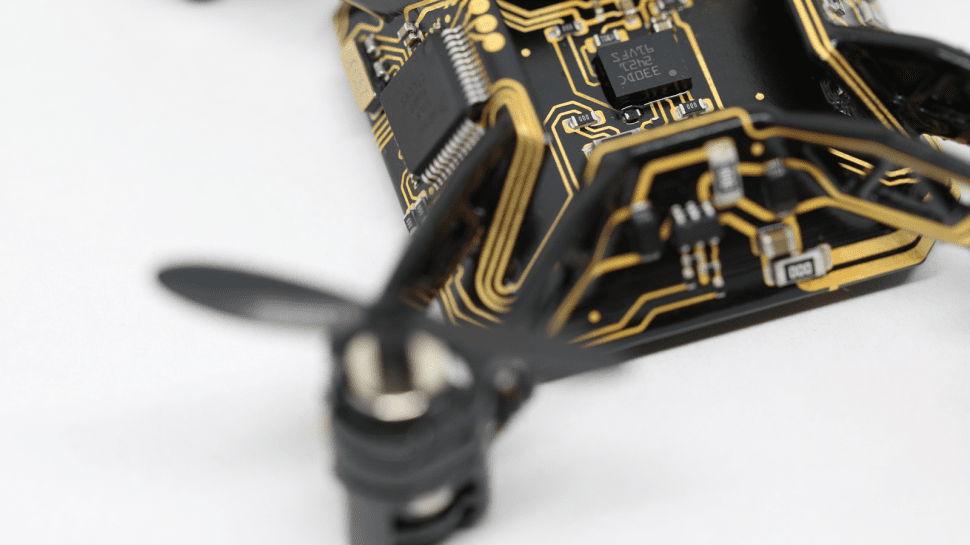
- Integration of additional functions for plastic parts (antennas, RFID elements, switches, shields, stitch connectors…)
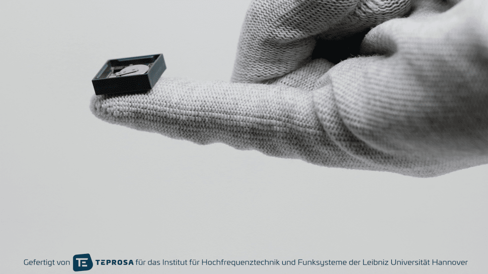
- High degree of miniaturization possible
- Reduction of assembly costs, for example through monolithic integration
- Prototype production cost-effective and fast in 3D printing process
The use of innovative technologies for manufacturing the base bodies, such as 3D printing, and the use of new substrate materials enable ever more functionalities and increasingly expand the possibilities of MID technology.
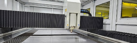
Manufacturing of 3D-MID
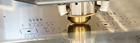
Various manufacturing options exist for the production of 3D-MID. In addition to 2C injection molding, the laser resist method and hot stamping, the LPKF LDS method (laser direct structuring) developed by the German mechanical engineering company LPKF Laser&Electronics AG is one of the most common methods for manufacturing mechatronic integrated devices. We manufacture exclusively using the LPKF-developed method and the laser resist method.
The production of 3D-MID using the LPKF method is carried out in a process chain with the following four basic process steps:
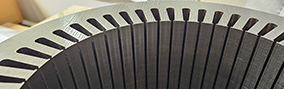
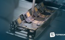
Base body generation (injection molding, 3D printing)
In the first process step, the base body is created that will later be used as a circuit carrier. Plastics (mostly thermoplastics) provided with special additives are used for this purpose. These plastics are processed by injection molding and increasingly by 3D printing.
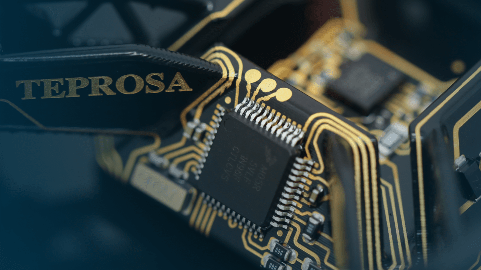
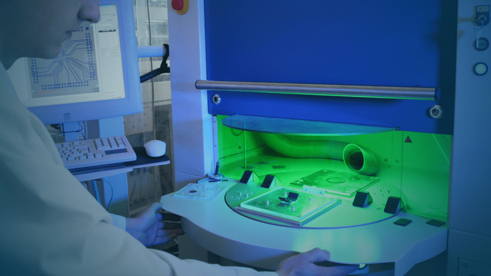
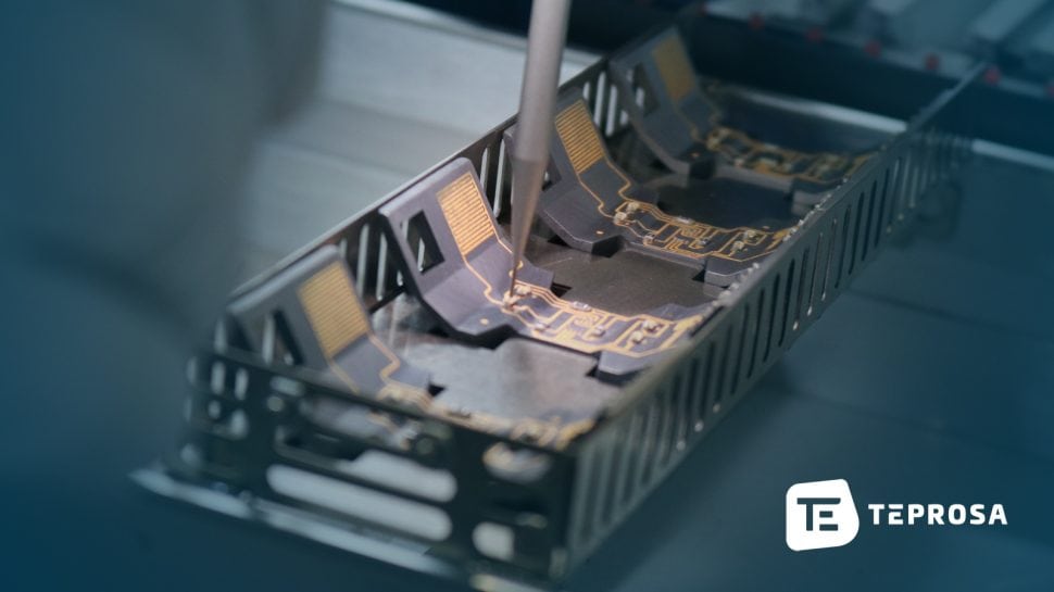
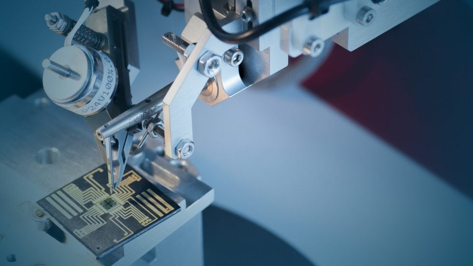
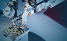
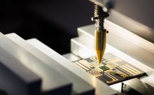
Laser direct structuring of 3D-MID
Laser direct structuring “exposes” the special additives contained in the plastic. The method used for this was developed by LPKF Laser & Electronics AG. During ablation of the top injection molding skin, the nuclei underneath are activated by the laser beam and thus modified for subsequent metal adhesion.
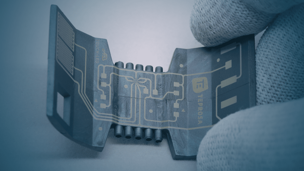
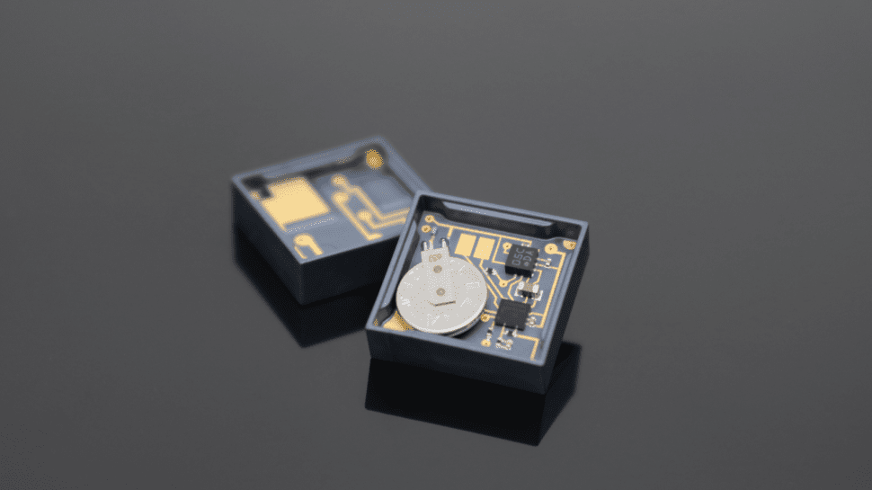
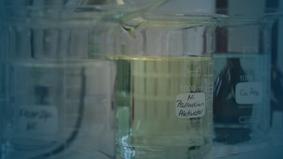
Metalization of 3D-MID
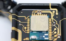
The plastic bodies modified by laser direct structuring can be further processed chemically or galvanically in special metallization processes. The additives exposed during structuring serve as seedlings for copper particles in the chemical metallization process step. In this way, an initial conductive layer is created, which can be reinforced in further metallization processes or supplemented with other metals (e.g. nickel, gold). In chemical metallization, metallization is performed without current, while in galvanic metallization the components are electrically contacted. In this way, even higher layer thicknesses can be achieved during metallization. The most commonly used layer structure consists of a layer of copper, followed by a layer of nickel and a final layer of gold (flash gold).
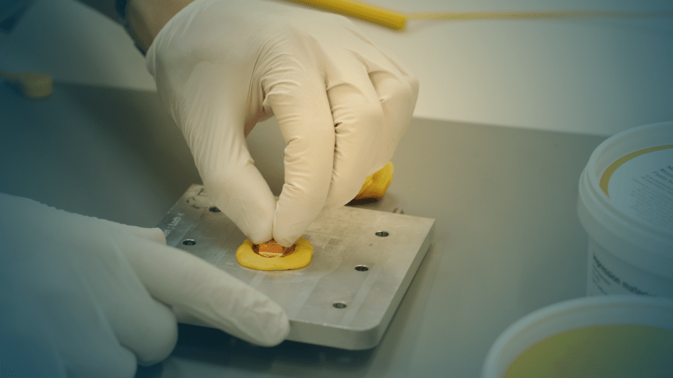
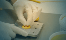
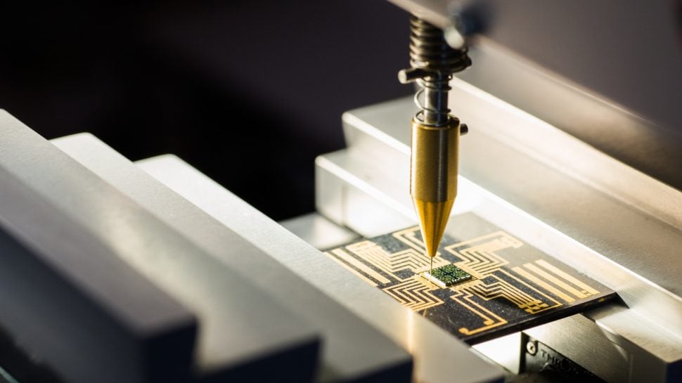
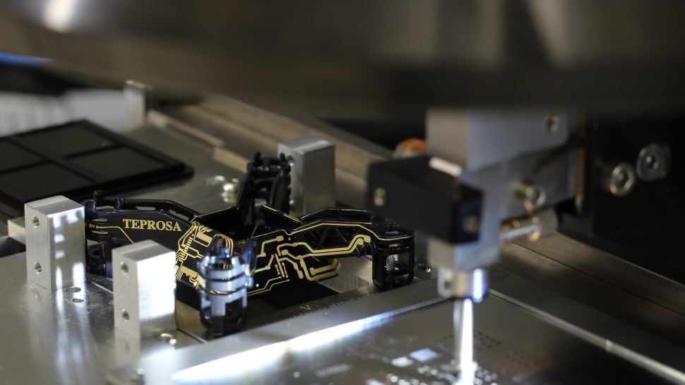
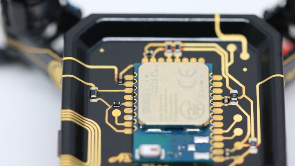
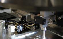
Equipping three-dimensional circuit carriers
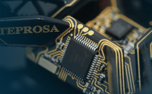
In the final process step of manufacturing an MID, the molded interconnect devices can be populated with electronic components. In principle, MIDs can be assembled according to the same principle as conventional circuit boards.
However, the assembly of the three-dimensional circuit carriers presents a particular challenge if many components are to be placed on different levels of the MID assemblies, resulting in a complex component design. In series production, however, inefficiencies caused by an unnecessarily complex component design or an incompletely thought-out placement of the individual components quickly become a major cost driver.
Prototyping and feasibility studies for 3D MID
When applying MID technology, there are many details to consider right from the start. Keeping the challenges of subsequent manufacturing in mind from the initial design of the 3D body can have a significant impact on the economics and performance of the eventual MID. Read our blog to find out where the most important pitfalls lurk and what to pay particular attention to.
Our quality management
As a service provider for the manufacturing of Mechatronic Integrated Devices, we have set ourselves the goal of manufacturing products with the highest quality standards. To achieve this goal, we work within the framework of our quality management system according to clearly defined processes, which we constantly review and develop. For us, quality does not only refer to the products, but to all business processes. You can find more information about our quality management system and processes here.
The Research Association 3-D MID e.V.
TEPROSA is a member of the Research Association 3 D-MID and also participates in the orientation of research on the topic of Mechatronic Integrated Devices within the framework of the Research Advisory Board.


