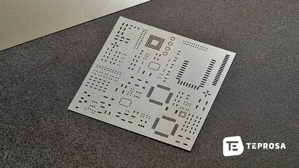
Manufacturing of SMD stencils
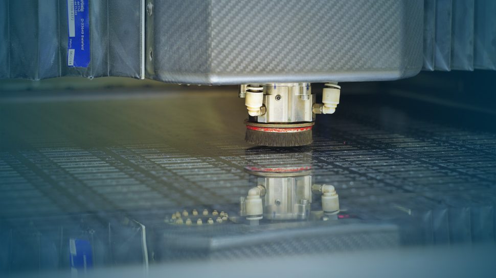
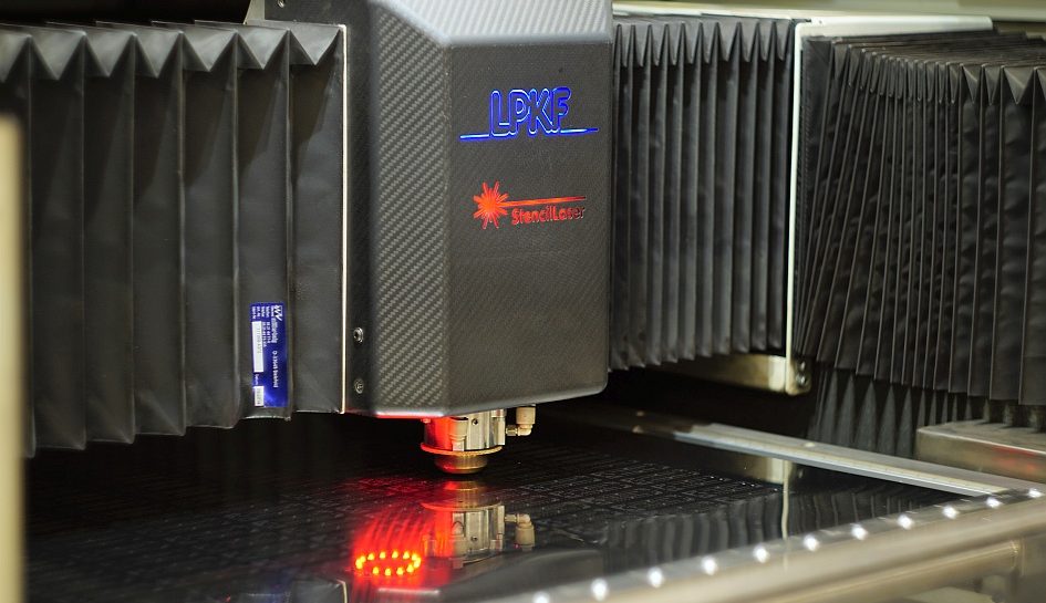
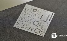
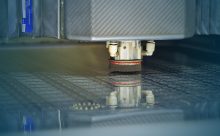
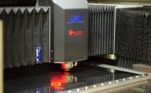
We have been manufacturing high-precision SMD stencils for all common quick clamping systems and in individual designs since 2012. For production, we rely on six LPKF G6080 laser systems of the latest generation. Due to the high capacity of each individual system, we are able to process your request immediately and deliver the stencils within the shortest possible time (express service within a few hours). The G6080 systems, which carry the epithet Stencil Laser, are predestined for the precise and fast processing of thin metal foils and are therefore especially suitable for the production of SMD stencils. Even step stencils, so-called stepstencils can be produced with the G6080 using a process specially developed by LPKF for this purpose.
Below you will find a short list of our possibilities in the production of SMD stencils. If you are still missing information for your inquiry, or you need further details, just ask. We will be happy to work out a joint solution for your project with you.
Our capabilities:
- Material: We use high quality starting material with low residual stress, high flatness as well as low thickness tolerance (2%) for SMD stencil production.
- Material thickness: 70µm- 200µm
- Stencil size: 800 mm x 600 mm
- Laser marking: stencil marking/marking (text), registration marks, feducials
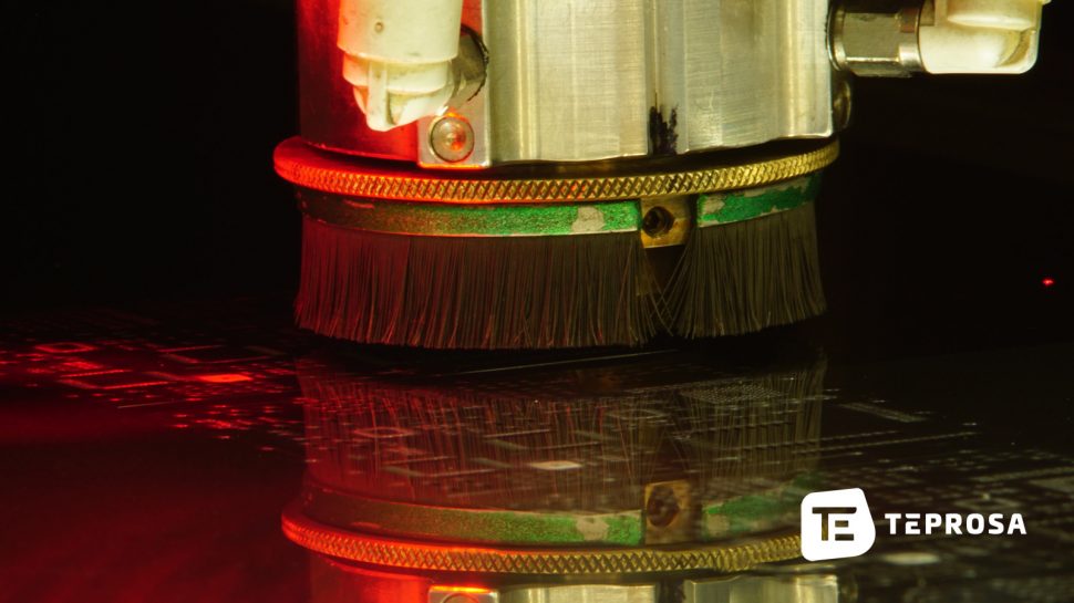
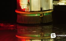
- Final treatment: brushing, electropolishing, nano-coating (Nanoclear)
- Data customization: changing pad geometries, rounded corners, length or area scaling, layout or part mirroring, panel creation
- Data optimization: optimization suggestions, determine pad areas, send approval documents in GERBER, PDF or jpeg format, material thickness adjustment suggestions, etc.
- Template production for a wide variety of stenter frame systems: ZelFlex Z4P, ZelFlex Protect, ZelFlex QR, DEK VectorMount, DEK VectorGuard, Beta QTS, Essemtec and many more. on request also special formats
We offer our customers individual advice and flexible service and of course handle small requests and special requests flexibly and with the utmost attention. Depending on the customer’s request, we take over the pad customization, or adhere entirely to your specifications. We are interested in a long-term partnership and want to understand what is important for you, so that we can fully consider your wishes.
JUST SEND US YOUR INQUIRY DATA
Just send us your inquiry data (alt. minimum details: Size, thickness, number of pads, quick release frame or individual design), the required number of pieces and the source material and we will send you an appropriate offer within the shortest possible time. Alternatively, you are of course welcome to contact us directly if there is still a need for consultation. Let’s go…
SURFACE FINISHING AND NANO COATING
We brush our SMD stencils from both sides as standard to further improve the SMD stencil properties and optimize your doctoring process. If desired, we also offer a cost-effective technique for fluxophobic (paste-repellent) stencil coating. NanoClear coating increases cleaning efficiency and reduces the required cleaning frequency. The adhesion of solder and flux is reduced, so that possible carry-over is avoided.
CONCLUSION
TEPROSA manufactures high precision laser cut SMD stencils for solder paste printing. State-of-the-art laser technology, innovative coating processes and comprehensive quality management guarantee the highest quality for optimal assembly of your PCBs. We accept any ideas and customer requests so that we can also find a suitable implementation for your project.
We look forward to hearing from you. Either via anfrage@teprosa.de or simply call us at +49 391 838177 90.


