
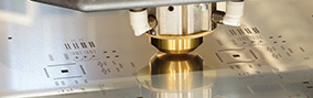
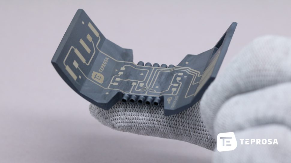
LASER DIRECT STRUCTURING (LPKF LDS PROCEDURE)
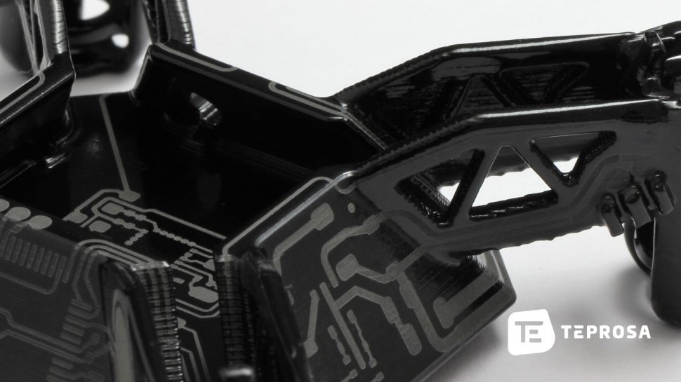
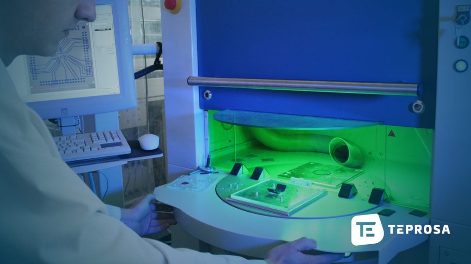
We offer laser direct structuring (LPKF-LDS process) for the production of 3D-MID (so-called three-dimensional circuit carriers) as a service in Magdeburg. 3D-MID stands for Mechatronic Integrated Device (or Molded Interconnected Devices). The MID technology makes it possible to use three-dimensional plastic parts as circuit carriers for electronic or mechatronic assemblies. The LPKF-LDS process is one of the technologically leading and at the same time most economically interesting process for the production of 3D-MID. The LPKF LDS process represents the central process step. The process was developed and patented by the company LPKF Laser & Electronics AG in Hanover. In laser direct structuring, special LDS additives contained in the plastic are exposed and thus activated. These additives serve in the subsequent process step, the chemical metallization as a seedling for copper particles. In this way, a first conductive layer is formed, which can be amplified in further metallization processes, or supplemented with other metals (e.g., nickel, gold). Following the metallization equivalent to the circuit board electrical components can be equipped. The result is a three-dimensional circuit carrier that, in addition to more freedom in design, also enables cost advantages and a higher functional density. TEPROSA offers you all process steps of the MID technology as a complete supplier and one of the few in Germany for the LPKF-LDS procedure Authorized Manufacturer.
OUR CAPABILITIES
- Method: LPKF-LDS method, laser resist method
- Possibilities of 3D-MID technology: project management, body procurement, LDS (laser direct structuring), laser resist process, chemical metallization, AVT / assembly
- Materials: Plastic (ABS, PC / ABS, PC, PA / PPA, PBT, COP, PPE, LCP, PEI, PEEK, PPS)
- Repeat accuracy: ± 2 μm
- Quantity: samples (from 1 part), small series, series
YOUR ADVANTAGES
- High design and design freedom for the development of electronic components
- Function integration for plastic parts (antennas, RFID elements, switches, shields, connectors and more)
- miniaturization
- Through connections possible
- Reduction of assembly costs through monolithic integration
- Suitable for samples, single pieces and small quantities – low set-up costs
We are happy to produce a free sample according to your specifications to convince you of our quality!
JUST SEND US YOUR ENQUIRY DATA
Just send us your desired marking or your data (STEP (.stp, .step), IGES (.igs, .iges) DXF (.dxf)), the requested quantity and the starting material and we will send you a corresponding one within a short time Offer. Alternatively, you are also welcome to contact us directly if there is any need for clarification. Let’s get started…
YOU MIGHT ALSO BE INTERESTED IN
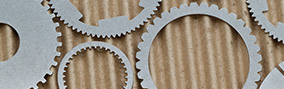
In addition to laser direct structuring as a service, we also offer, among other things, the production of fineblanked parts made of fine and thin sheet metal. In addition to laser fineblanking, drilling, and marking, our services also include the ablation of individual layers. Of course, the combination of different methods is possible. Just contact us.
Do you already know our services in the areas
- Laser finishing
- Chemical metallization
- AVT / placement of 3D-MID
- Testing and testing 3D-MID
- Motor and engine mounts


