3D-MID technology for the selective coating of plastic parts
With the help of the 3D-MID process, plastic parts can be metallized not only over the entire surface, but also selectively. To do this, the plastic part is activated with a special laser at the points that are to be coated (this is referred to as laser activation or laser direct structuring). The additives contained in the plastic directly under the plastic surface are “exposed” by the laser treatment.
In a chemical bath, copper particles can then be deposited specifically only on the activated surfaces. Other metals, e.g. nickel, tin or gold, can then be deposited onto the starting layer of copper. In this way, a selectively coated plastic part is obtained.
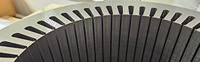
MID technology thereby makes it possible to selectively coat two-dimensional and also three-dimensional plastic parts and use them, for example, as circuit carriers for electronic or mechatronic assemblies. With the LPKF-LDS process, metallic conductor paths are applied to the substrate material, creating three-dimensional assemblies that also serve as circuit carriers.
These spatial electronic assemblies are manufactured using 3D-MID technology and, compared to conventional assemblies, enable the integration of electronic, mechanical, fluidic, optical and thermal functions. The resulting additional benefits represent advantages that cannot be realized with two-dimensional circuit carriers (printed circuit boards).
But not only circuit carriers can be produced with the process. The ability to selectively coat plastics with metal also enables the production of antennas, shielding or decorative surfaces, among other things.
TEPROSA offers you the entire 3D MID production chain from a single source as a full-service provider. If external processes are necessary for the production of your MID, we will gladly take over the supplier management, so that you can fully concentrate on your product.
Materials for selective metallization
Plastics containing the LDS additive developed by LPKF Laser & Electronics AG are suitable for selective metallization using 3D MID technology. There are now a large number of laser-activatable thermoplastics that contain the necessary metallic additive and are therefore suitable for the production of MIDs using LPKF’s laser direct structuring process. Here you will find a selection of the basically available polymers:
- PC (polycarbonate)
- PC + PET (polycarbonate (PC) with the properties of polyethylene terephthalate (PET))
- PC/ABS (polycarbonate (PC) with the properties of acrylonitrile butadiene styrene (ABS))
- PA/PPA (polyamide (PA) with the properties of polyphate halamide (PPA))
- PA6 (polyamide 6)
- PPA (polyphathalamide)
- PA4 (polyamide 4)
- PA66 (polyamide 66)
- LCP (Liquid Crystal Polymer)
- PEEK (Polyetheretherketone)
- PPS (polyphenylene sulfide)
- PET (polyethylene terephthalate)
- PEI (polyetherimide)
- PBT (polybutylene terephthalate)
- PET + PBT (polyethylene terephthalate)
- COP (Cyclic Olefin Polymer)
- PPE (Polyphenylene Ether)
In principle, it is possible to add the LDS additive to a plastic. We are happy to advise you on the selection of plastic granules, the appropriate process and take over the procurement for you. A selection of common plastic granules we always have in stock, so we can start immediately with your project.
Selective metallization of additively manufactured plastic parts
Additively manufactured plastic parts are also suitable in principle for selective coating using the 3D-MID process. Printable filaments and resins now exist that can be used in both FDM and SLA printing. Parts produced in this way can be activated and chemically selectively metallized using the LPKF LDS method.
Production of a plastic metallization
The production of a plastic metallization using the LPLF method is carried out in a process chain with the following four basic process steps:
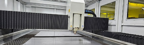
Base body generation (injection molding, 3D printing)
In the first process step, the base body is generated, which is to be metallized later. Plastics (mostly thermoplastics) provided with special additives are used for this purpose. These plastics are processed by injection molding and increasingly by 3D printing.
Selective laser activation
Laser activation (laser direct structuring) “exposes” the special additives contained in the plastic. The process used for this purpose was developed by LPKF Laser & Electronics AG. During ablation of the top injection molding skin, the nuclei underneath are activated by the laser beam and thus modified for subsequent metal adhesion.
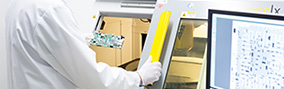
Coating process / metallization
The coating of the plastic parts after laser activation takes place in special metallization baths. The additives exposed during activation serve as seedlings for copper particles in the chemical metallization process step. In this way, an initial metal layer is created, which can be reinforced in further metallization processes or supplemented with other metals (e.g. nickel, tin, gold). One possibility of adding larger layer thicknesses is plastic electroplating.
Use of metallized plastic parts as circuit carriers
Once the coating has been applied, the modified plastic parts can also be used as circuit carriers and fitted with electronic components. They are then referred to as mechatronic integrated devices/MIDs. In principle, MIDs can be assembled in the same way as conventional printed circuit boards.
However, the assembly of three-dimensional circuit carriers poses a particular challenge if many components are to be placed on different levels of the MID assemblies, resulting in a complex component design. In series production, however, inefficiencies caused by an unnecessarily complex component design or an incompletely thought-out placement of the individual components quickly become a major cost driver.


