


Phone consultation: +49 391 598184 70
Email: anfrage@teprosa.de
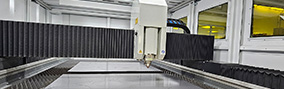
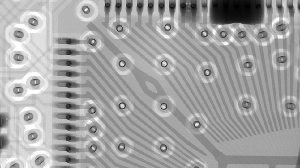
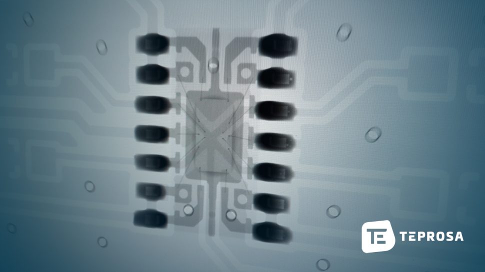
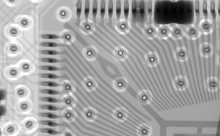
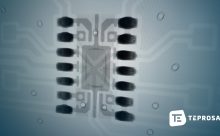
X-ray inspection of electronic assemblies and electronics
X-ray inspection provides a non-destructive means of analyzing printed circuit boards and other electronic assemblies in the electronics industry, particularly in the assembly of printed circuit boards. It is frequently used in quality control during production and development.
Testing laboratory for X-ray testing, analysis and inspection of electronic components
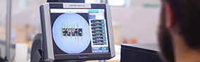
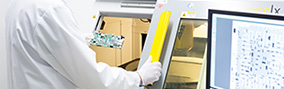
We specialize in testing electronic assemblies and have a lot of experience with the requirements of the electronics and automotive industries. On behalf of our customers, we produce high-resolution X-ray images of solder joints and individual components, making weak points visible.
We will be happy to advise you regarding your inspection tasks.
What are the advantages of X-ray of electronics?
- Destruction-free inspection method of solder joints / solder connections and components
- High resolution images
- Optional: CT images (3D computed tomography)
Which tests can we perform?
Here is an overview of the most common tests we can offer in the field of component and failure analysis in our testing laboratory.
- Inspection of electrical components of any kind
- 2D X-ray testing
- CT analyses
- X-ray testing according to DIN EN ISO/IEC 17025
Advantages of an X-ray examination at TEPROSA
- Exceptionally good image quality
- Fast processing of your samples
- Creation of a meaningful test report
- Evaluation based on previously agreed criteria
- Further testing and advice available directly from TEPROSA
How long does an X-ray inspection take?
Depending on the sample size, the normal processing time of a test order for X-ray at TEPROSA is 1-3 working days. We will be happy to check the possibility of express processing for you. For the creation of a test report, we need another 1-3 working days, depending on the scope.